Table of Contents
1. Introduction & Overview
Flexible electronics represent a paradigm shift from rigid, silicon-based systems towards lightweight, conformable devices for wearable health monitors, foldable displays, and epidermal sensors. A critical bottleneck has been the conductive material for interconnects. Indium Tin Oxide (ITO), the incumbent standard, is fundamentally brittle and suffers from indium scarcity. This paper by Baig and Abe presents a compelling alternative: electrically interconnected Platinum (Pt) nanonetworks fabricated via a controlled atmospheric treatment that induces nanophase separation in a Pt-Ce alloy thin film. The core innovation lies in achieving a percolating network of Pt with exceptional mechanical durability (surviving 1000+ bending cycles down to 1.5 mm radius) while maintaining a functional sheet resistance (~2.76 kΩ/sq).
Key Performance Metric
~2.76 kΩ/sq
Sheet resistance after 1000 bending cycles
Mechanical Durability
>1000 cycles
Bending cycles at 1.5 mm radius
Film Thickness
< 50 nm
Average thickness of Pt nanonetwork
2. Methodology & Fabrication Process
The fabrication strategy is elegantly simple, avoiding complex lithography. It hinges on a two-step process: deposition followed by a reactive atmospheric treatment.
2.1 Substrate Preparation & Alloy Deposition
A 50 nm-thick film of a Platinum-Cerium (Pt-Ce) alloy is deposited onto a flexible polyimide (PI) substrate using standard physical vapor deposition (e.g., sputtering). The choice of PI is crucial for its high thermal stability and inherent flexibility.
2.2 Atmospheric Treatment & Phase Separation
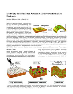
The deposited film is subjected to an elevated temperature treatment in an atmosphere containing Carbon Monoxide (CO) and Oxygen (O₂). This is the critical step that drives the nanophase separation. The treatment oxidizes Cerium (Ce) into insulating Cerium Dioxide (CeO₂), while the Platinum (Pt) aggregates and forms an interconnected, percolating nanonetwork structure. The paper identifies precise temperature and time thresholds: lower temperatures/shorter times yield interconnected networks, while higher temperatures/longer times lead to disconnected Pt nanoislands.
Schematic Description (Fig. 1): The figure illustrates a device with the Pt-Ce alloy deposited on PI. After the CO/O₂ treatment, a nanotexture emerges where red, web-like structures (Pt nanonetworks) are embedded within a green matrix (CeO₂) on the substrate.
3. Results & Characterization
3.1 Structural Analysis (SEM/TEM)
Scanning/Transmission Electron Microscopy (SEM/TEM) imaging confirms the formation of the nanonetwork. The interconnected Pt pathways are visually distinct from the CeO₂ background, with feature sizes on the nanometer scale, contributing to the material's flexibility.
3.2 Electrical Performance & Bending Tests
The electrical stability is the standout result. The Pt nanonetworks on PI maintain a sheet resistance of approximately 2.76 kΩ/sq even after 1000 bending cycles at varying diameters, down to an extreme bending radius of 1.5 mm. This demonstrates superior durability compared to ITO, which typically cracks under far less strain.
3.3 LCR Measurements & Electrical Response
Inductance, Capacitance, and Resistance (LCR) measurements reveal a fascinating structure-property relationship:
- Interconnected Pt Nanonetworks: Exhibit inductor-like electrical responses. This suggests a continuous, percolating conductive path where current flow induces a magnetic field.
- Disconnected Pt Nanoislands: Display capacitor-like behavior. This indicates isolated conductive islands separated by insulating gaps (CeO₂), forming a distributed capacitor network.
4. Technical Details & Mathematical Models
The performance can be contextualized using percolation theory, which models how connectivity emerges in random networks. The sheet resistance $R_s$ of a thin film is given by $R_s = \rho / t$, where $\rho$ is resistivity and $t$ is thickness. The nanonetwork's effective resistivity is governed by the percolation threshold and the tortuosity of the Pt pathways. The phase separation kinetics likely follow an Arrhenius-type relationship, where the treatment time $t$ and temperature $T$ determine the degree of phase separation: $\text{Phase Separation Rate} \propto \exp(-E_a / k_B T)$, where $E_a$ is the activation energy and $k_B$ is Boltzmann's constant. Exceeding a critical $T \times t$ product pushes the system from the interconnected network regime into the disconnected nanoisland regime.
5. Analysis Framework & Case Study
Framework for Evaluating Flexible Conductor Technologies:
- Material & Process Scalability: Assess cost, material availability (Pt vs. In), and fabrication complexity (lithography-free vs. multi-step lithography).
- Mechanical-Electrical Durability: Quantify performance (sheet resistance) under cyclic mechanical stress (bending, stretching). Define failure criteria (e.g., 20% increase in $R_s$).
- Functional Versatility: Evaluate beyond simple conductivity (e.g., LCR response, transparency, biocompatibility).
- Integration Readiness: Compatibility with standard semiconductor/flexible electronics fabrication processes.
6. Critical Analysis & Expert Interpretation
Core Insight: Baig and Abe aren't just presenting another flexible conductor; they're demonstrating a materials processing hack. By leveraging the thermodynamic instability of a Pt-Ce alloy under a specific reactive atmosphere, they "program" a self-organizing, durable conductive network. This moves beyond patterning (like lithography) into the realm of controlled material genesis, reminiscent of how phase separation principles guide structure in block copolymers (as explored in materials science journals like Advanced Materials).
Logical Flow: The argument is solid: 1) ITO is flawed (brittle, scarce). 2) Existing metal mesh solutions are complex. 3) Here's a simple, lithography-free alternative. 4) The key is controlling phase separation via T/t. 5) The result is mechanically robust and electrically interesting (LCR response). The link between process parameters (T, t), microstructure (connected vs. islands), and macro-property (inductive vs. capacitive) is particularly elegant and well-supported by data.
Strengths & Flaws:
- Major Strength: The process simplicity and the clear process-structure-property relationship. The use of LCR as a microstructural diagnostic is clever.
- Critical Flaw: The elephant in the room is cost and sheet resistance. Platinum is orders of magnitude more expensive than ITO or even silver inks. A sheet resistance of ~2.8 kΩ/sq, while stable, is too high for many display or high-frequency interconnect applications. It's suitable for sensors or low-current applications, which the paper tacitly admits by focusing on flexibility over absolute conductivity.
- Missing Data: Transparency (critical for displays) is not discussed. Long-term environmental stability (oxidation of Pt nanoscale features?) is unaddressed.
Actionable Insights:
- For Researchers: The core concept—using atmospheric treatment to drive phase separation in alloy films—is highly generalizable. Immediately investigate other alloy systems (e.g., Au-Zr, Ag-Ce) to find a cheaper, more conductive, or more transparent analogue. Explore stretching tolerance, not just bending.
- For R&D Managers: This technology is not an ITO killer for displays. Its near-term niche is in high-reliability, niche flexible sensors where performance stability justifies Pt cost (e.g., medical, aerospace, or ruggedized wearable devices). Prioritize applications where 2.8 kΩ/sq is acceptable.
- For Investors: Cautious optimism. The scientific merit is high, but commercial viability hinges entirely on finding a non-Pt alloy system or demonstrating a unique, high-value application where its durability is irreplaceable. Watch for follow-up papers on alternative materials.
7. Future Applications & Development Directions
- Biomedical Implants & Chronic Wearables: The combination of Pt's biocompatibility and the network's mechanical durability is ideal for long-term neural interfaces, pacemaker leads, or implantable glucose sensors that must flex with organ movement.
- Ruggedized Flexible Circuits: Applications in aerospace (conformal antennas on drone wings), automotive (sensors on flexible joints), or industrial robotics where extreme and repeated flexing is required.
- Multifunctional Skins: Leveraging the LCR response, the nanonetwork could act as both a strain sensor and a passive electrical component (inductor/capacitor) in a single, flexible layer, enabling novel circuit designs for soft robotics.
- Material System Expansion: The most critical future direction is applying this atmospheric phase-separation principle to other metal-oxide systems (e.g., Silver-based, Copper-based) to drastically reduce cost and potentially improve conductivity.
- Integration with Stretchable Substrates: Moving from bendable (PI) to stretchable substrates (e.g., PDMS, SEBS) to enable truly elastic electronics.
8. References
- Baig, S. M., & Abe, H. (Year). Electrically Interconnected Platinum Nanonetworks for Flexible Electronics. [Journal Name, Volume, Pages].
- Dong, et al. (Year). Laser interference lithography of ITO nanopatterns for flexible electronics. Nano Letters.
- Seo, et al. (Year). Gold nanomesh for electrophysiology. Nature Nanotechnology.
- Guo, et al. (Year). Au nanomesh via grain boundary lithography. Advanced Functional Materials.
- Adrien, et al. (Year). Chemical fabrication of Au nanomesh on PET. Science.
- Bates, F. S., & Fredrickson, G. H. (1999). Block Copolymers—Designer Soft Materials. Physics Today. (For phase separation principles).
- Kim, D.-H., et al. (2010). Epidermal Electronics. Science. (For context on flexible, skin-integrated devices).
- Web Source: National Institute of Standards and Technology (NIST) - Materials for Flexible Electronics. (For industry standards and challenges).