Electrically Interconnected Platinum Nanonetworks for Flexible Electronics: Fabrication, Characterization, and Applications
Analysis of a novel method for fabricating flexible, electrically interconnected platinum nanonetworks on polyimide substrates via atmospheric treatment of Pt-Ce alloy films.
Home »
Documentation »
Electrically Interconnected Platinum Nanonetworks for Flexible Electronics: Fabrication, Characterization, and Applications
1. Introduction & Overview
Flexible electronics represent a paradigm shift in device design, enabling lightweight, bendable, and conformable systems for applications ranging from wearable health monitors to foldable displays. A critical bottleneck in this field has been the development of durable, high-performance conductive materials. While Indium Tin Oxide (ITO) has been the industry standard, its inherent brittleness and the scarcity of indium limit its viability for applications requiring repeated mechanical deformation.
This work introduces a novel alternative: electrically interconnected Platinum (Pt) nanonetworks fabricated on flexible polyimide (PI) substrates. The core innovation lies in a fabrication process that leverages atmospheric treatment to induce nanophase separation in a deposited Platinum-Cerium (Pt-Ce) alloy thin film. This process creates a percolating network of Pt nanowires embedded within an insulating Cerium Dioxide (CeO₂) matrix, resulting in a material that combines exceptional mechanical flexibility with stable electrical conductivity.
2. Methodology & Fabrication Process
The fabrication of Pt nanonetworks is a two-step process designed for simplicity and potential scalability.
2.1 Substrate Preparation & Alloy Deposition
A thin film (approximately 50 nm) of a Platinum-Cerium (Pt-Ce) alloy is deposited onto a clean polyimide (PI) substrate using a physical vapor deposition technique, such as sputtering. The choice of PI is crucial due to its high thermal stability and excellent mechanical flexibility.
2.2 Atmospheric Treatment & Phase Separation
The deposited alloy film is then subjected to a controlled atmospheric treatment at elevated temperatures. The treatment environment consists of a gas mixture of Carbon Monoxide (CO) and Oxygen (O₂). This treatment is the key to the process:
Chemical Driver: CO acts as a reducing agent for Pt, while O₂ oxidizes Cerium (Ce).
Phase Separation: The differential reactivity drives the nanophase separation of the alloy. Pt coalesces into a continuous, interconnected nanowire network, while Ce is oxidized to form insulating CeO₂ nanoparticles that occupy the spaces between the Pt network.
Parameter Control: The temperature and duration of this treatment are critical. Lower temperatures/shorter times favor interconnected networks, while higher temperatures/longer times lead to isolated Pt nanoislands.
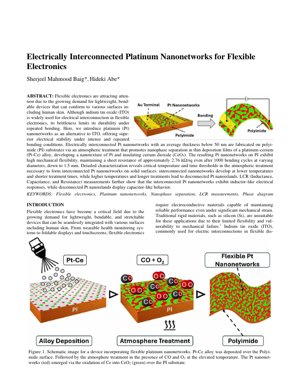
Visual Reference: Figure 1 in the PDF provides a schematic of this process, showing the transformation from a uniform Pt-Ce film to a textured Pt (red network) and CeO₂ (green) structure on PI.
3. Results & Characterization
3.1 Structural & Morphological Analysis
Microscopic analysis (e.g., SEM, TEM) confirms the formation of a nanotexture. The Pt forms a percolating, web-like network with feature sizes on the nanoscale. The CeO₂ forms a discontinuous, insulating phase. The study successfully maps a processing "phase diagram," identifying the precise temperature-time windows that yield interconnected networks versus disconnected islands.
3.2 Electrical & Mechanical Performance
Key Performance Metric
~2.76 kΩ/sq
Sheet Resistance maintained after 1000 bending cycles
Mechanical Robustness
1.5 mm
Minimum bending diameter tested
The Pt nanonetworks demonstrate remarkable mechanical durability. The sheet resistance remains stable at approximately 2.76 kΩ/sq even after 1000 bending cycles at various diameters, down to a tight radius of 1.5 mm. This performance starkly contrasts with ITO, which typically cracks and fails under similar conditions.
3.3 LCR Measurements & Electrical Response
Impedance spectroscopy (LCR measurements) reveals a fundamental difference in the electrical behavior based on morphology:
Interconnected Nanonetworks: Exhibit an inductor-like frequency response. This suggests a continuous conductive path where current flow is dominated by the inductive properties of the wire-like Pt network.
Disconnected Nanoislands: Display capacitor-like behavior. This is characteristic of discontinuous metal islands separated by insulating gaps (CeO₂), forming a distributed capacitor network.
This electrical signature serves as a powerful diagnostic tool to confirm the successful formation of the intended interconnected structure.
4. Technical Details & Mathematical Models
The electrical properties of the nanonetwork can be modeled using percolation theory and effective medium approximations. The sheet resistance $R_s$ is governed by the connectivity of the Pt network. For a 2D percolating network near the percolation threshold, it can be described by:
$R_s \propto (p - p_c)^{-t}$
where $p$ is the volume fraction of Pt, $p_c$ is the critical percolation threshold, and $t$ is a critical exponent (typically ~1.3 for 2D). The atmospheric treatment directly controls $p$ and the connectivity, thereby tuning $R_s$.
The inductor-like behavior arises from the self-inductance $L$ of the nanoscale wire loops within the network: $Z_L = j\omega L$, where $\omega$ is the angular frequency. The capacitor-like behavior in island structures comes from the junction capacitance $C$ between islands: $Z_C = 1/(j\omega C)$.
5. Analysis Framework & Case Example
Framework for Evaluating Novel Flexible Conductors:
Material & Process Scalability: Assess the complexity, cost, and environmental impact of the fabrication method (e.g., vs. lithography).
Performance Benchmarking: Quantify electrical conductivity ($R_s$) and mechanical stability (cycles-to-failure, minimum bend radius) against benchmarks (ITO, Ag nanowires, graphene).
Morphology-Function Correlation: Use characterization (SEM, LCR) to link nanostructure (interconnected vs. island) to macroscopic electrical properties.
Application-Specific Suitability: Map performance metrics to target application requirements (e.g., wearable sensors need low $R_s$ and high flexibility).
Case Example - Pt Nanonetwork vs. Competing Technology: Compare this Pt process to a standard Ag nanowire spray-coating method. While Ag nanowires may initially achieve lower $R_s$, they often suffer from poor adhesion, oxidation, and junction resistance instability under bending. The Pt nanonetwork, formed in-situ and partially embedded, likely offers superior environmental stability and junction robustness, albeit at a higher material cost. The analysis would weigh these trade-offs for a specific product, like a long-term implantable biosensor where stability trumps initial conductivity.
6. Future Applications & Development Directions
Near-term Applications:
Advanced Wearable Biosensors: For continuous, conformal health monitoring (ECG, EMG, sweat analysis) due to biocompatibility of Pt and flexibility.
Flexible Transparent Electrodes for OLEDs: If the network density and optical transparency can be optimized.
Strain & Pressure Sensors: Leveraging the predictable change in $R_s$ with mechanical deformation of the nanonetwork.
Future Research Directions:
Reducing Sheet Resistance: Exploring alloy compositions or post-treatment processes to enhance Pt connectivity and reduce $R_s$ towards ITO levels (<100 Ω/sq).
Transparency Optimization: Engineering the nanonetwork geometry (wire width, pitch) to balance conductivity and optical transmittance.
Stretchability: Integrating the nanonetwork into elastomeric substrates (e.g., PDMS) to achieve not just bendable but stretchable electronics.
Large-Area, Roll-to-Roll Fabrication: Adapting the atmospheric treatment for continuous, high-throughput manufacturing.
7. References
Rogers, J. A., Someya, T., & Huang, Y. (2010). Materials and mechanics for stretchable electronics. Science, 327(5973), 1603-1607.
Kim, D.-H., et al. (2011). Epidermal electronics. Science, 333(6044), 838-843.
Hu, L., Wu, H., & Cui, Y. (2011). Metal nanogrids, nanowires, and nanofibers for transparent electrodes. MRS Bulletin, 36(10), 760-765.
Dong, et al. (2020). Laser interference lithography for flexible ITO electrodes. Advanced Materials Technologies, 5(3), 1900934.
Seo, et al. (2018). Gold nanomesh for electrophysiology. Nature Nanotechnology, 13, 1048-1056.
Guo, et al. (2019). Fabrication of Au nanomesh on PDMS. ACS Nano, 13(2), 1549-1557.
Adrien, et al. (2021). Chemical fabrication of Au nanomesh on PET. Advanced Functional Materials, 31(15), 2008556.
National Institute of Materials Science (NIMS) Database on Flexible Electronics Materials.
8. Original Analysis & Expert Commentary
Core Insight
This paper isn't just about a new material; it's a masterclass in process-driven property engineering. The researchers have identified a sweet spot in materials processing—atmospheric treatment of a binary alloy—that directly dictates the nanoscale morphology (network vs. islands), which in turn programs the macro-scale electrical response (inductive vs. capacitive). This causal chain from process parameter to function is elegantly clear and represents a significant design principle for functional nanomaterials.
Logical Flow
The logic is compelling: 1) ITO fails mechanically. 2) Metal networks are a solution, but fabrication is complex. 3) Their solution: use a self-organizing chemical reaction (phase separation) to grow the network in-situ. 4) Prove it works with robust electrical and mechanical data. 5) Provide a deep physical explanation using LCR to link morphology to electronics. The flow from problem to synthetic solution to fundamental characterization is seamless.
Strengths & Flaws
Strengths: The methodology is notably simpler than multi-step lithography, offering a potential path to scalability. The mechanical durability data (1000 cycles at 1.5mm) is convincing and directly addresses ITO's Achilles' heel. Using LCR as a structural diagnostic tool is ingenious and provides high-value insight.
Critical Flaws: The elephant in the room is the sheet resistance of 2.76 kΩ/sq. This is orders of magnitude higher than ITO (~10-100 Ω/sq) or even other metal networks. For many display or high-frequency applications, this is a non-starter. The paper glosses over this, focusing on stability. Furthermore, the use of Platinum, a precious metal, raises serious cost and scalability concerns for consumer electronics, though it may be justifiable for niche medical devices. The process also requires elevated temperature, which may limit substrate choice.
Actionable Insights
For R&D teams: Pivot from Pt. The core innovation is the phase-separation mechanism. Immediate follow-up work should apply this atmospheric treatment paradigm to more abundant and conductive alloy systems (e.g., Cu-X, Ag-X) to slash $R_s$ and cost. For product developers: Target the right application. Don't try to replace ITO in displays yet. Instead, focus on markets where mechanical reliability is paramount and higher resistance is tolerable—think of implantable or long-term epidermal sensors, where Pt's biocompatibility is a major bonus. This technology's first commercial victory will be in a high-value, performance-critical niche, not the mass market.
This work reminds me of the early days of CycleGAN (Zhu et al., 2017) in computer vision. CycleGAN introduced an elegant, unsupervised framework for image-to-image translation by leveraging cycle consistency. Similarly, this paper introduces an elegant, in-situ framework for creating conductive networks by leveraging a self-limiting chemical reaction. Both are foundational in their approach, providing a new "template" for others to build upon and adapt with different materials (like swapping artistic styles in CycleGAN for different metal alloys here) to solve a broader set of problems.